Patterning technology for advancements in scaling
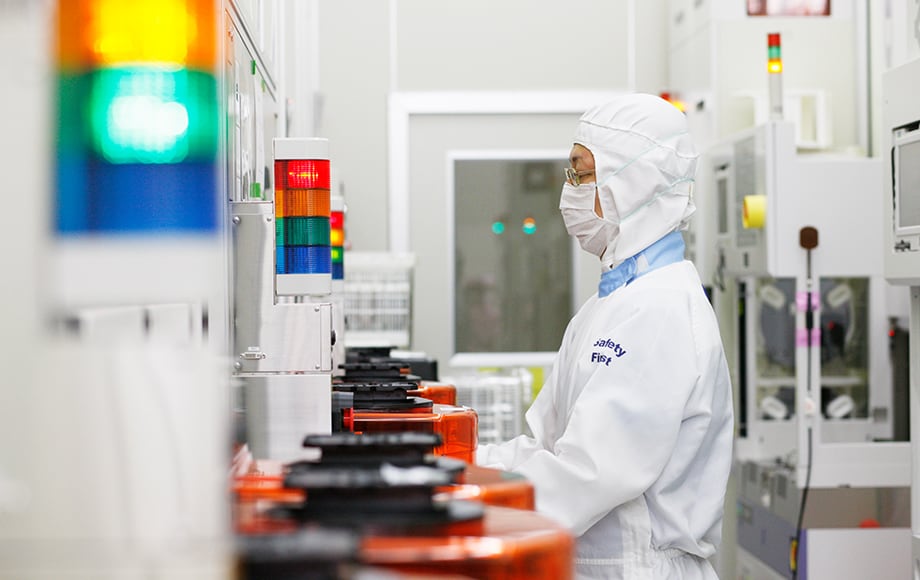
Semiconductor IC has been continuously scaled for the past 50 years, evolving its performance to be faster, less power consumption and less cost. Line width is about to fall below 20nm, and number of transistors is about to exceed hundred million within 1mm2. Tokyo Electron keep investing activity on developing a comprehensive patterning technology.
Evolution of semiconductor by scaling technology
Semiconductors have been scaling continuously for the past 50 years, evolving to perform faster, with less power consumption and lower cost. Line width is poised to fall below 20nm and the number of transistors will soon exceed several ten million per 1mm2
Wavelength of exposure tool has been the major driver to reduce minimum processing dimension. Continuous scaling has been enabled by shortening the wavelength from light source inside exposure tool. However, shortening of wavelength is becoming more and more difficult than ever from technology point of view, as well as cost point of view. ArF immersion technology was introduced in around 2006, and further evolution of exposure light source has not been introduced since then.
Extending ArF immersion lithography, patterning technology has been introduced to enable further scaling, by enhancing various process technologies such as deposition, coating, etch and clean. (Fig. 1)

Fig. 1 Scaling of semiconductor
Introduction of advanced patterning technology and challenges
“Multi-patterning technology” is the first approach introduced in the actual production processes. Single exposure process is decomposed into multiple exposure steps and combined at the later steps, enabling to exceed previous scaling limit of single exposure.
However, as the number of the decomposition increases, overlay errors are accumulated into larger number, and finally cause overall placement error to exceed its allowance. Moreover, allowance of the locational shift and deformation of substrates has become more critical than ever, along with the advance of scaling. For example, dimensional variation due to line edge roughness, line width roughness, pattern leaning or accumulation of those placement errors will all impact the process accuracy. (Fig. 2)
Multi-patterning technology by itself has now faced the limit of further scaling. Requirement to patterning has extended to self-alignment technology, in addition to multiple-patterning. Various advanced patterning approaches has been developed by revising device structure and process flow. Below are some example of patterning technologies implemented at metal line formation of actual production lines.
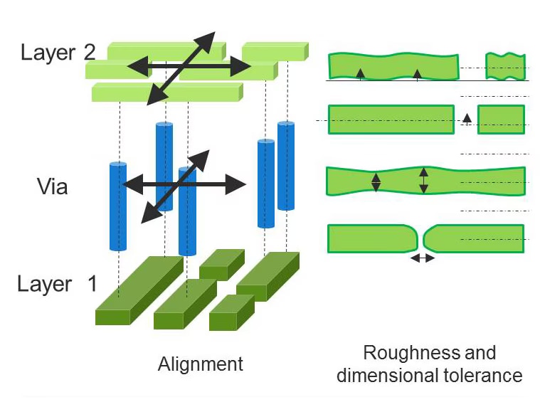
Fig. 2 Challenges at Patterning
SADP – Scaling by thin film formation on sidewall
SADP(Self-Aligned Double Patterning)is a technology to double the grid density (= half the pitch) formed by lithography.
First of all, grid structure is formed by exposure tool, and then thin and uniform film is covered all over the grid. Next, the film is fully removed except the film on sidewall of the grid. Finally the initial grid is removed, so only the thin film at the sidewall remains. Since the remaining film is originated from both side of the grid wall, new gird structure is formed with twice the density of walls from the original grid. (Fig. 3)
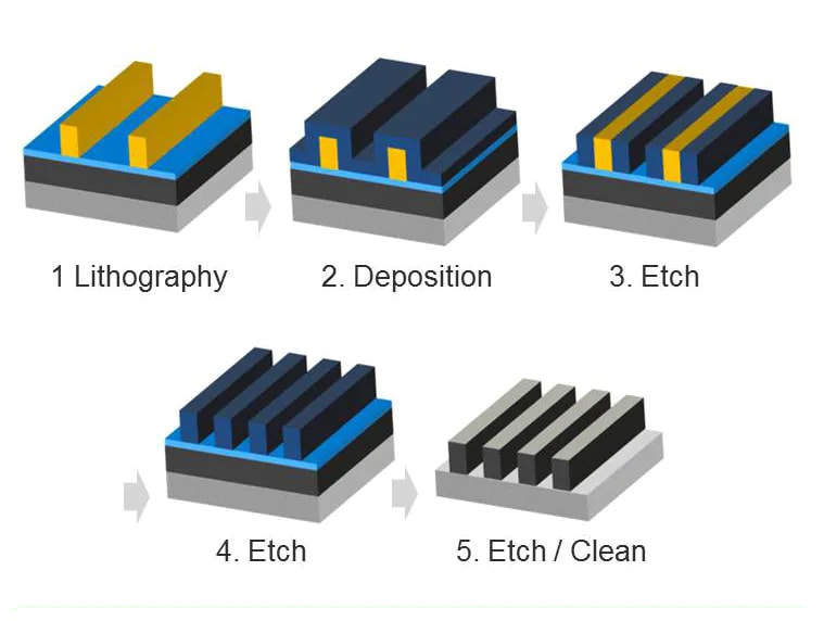
Fig. 3 SADP technology
SAQP – Scaling by extending SADP technology
SAQP (Self-Aligned Quadruple Patterning) is a technology to even double the density by repeating SADP processes (Fig. 4). If initial pitch of exposure tool is 80nm, SAQP enables to form 20nm pitch structure. Fine scaling is enabled by the collaboration of multiple processes; exposure, deposition, etch and clean.
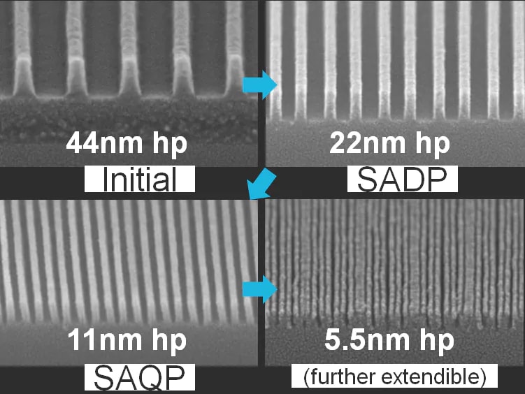
Fig. 4 Self-aligned multiple patterning
SAB – Scaling by etch selectivity to multiple materials
Fine grid structure has formed by SADP/SAQP technology. To transform the grid into circuit structure, the grid has to have cuts or blocks.
SAB (Self-aligned block) is a technology to form cut/block on grid pattern at precise accuracy. First of all, new grid is formed on top of the original grid at perpendicular direction. 3 different materials are used to structure the new grid. Next, mask of cut/block is formed on top of the new gird by exposure tool. Conventionally, high locational accuracy was required for the placement of this mask. By utilizing etch selectivity of the 3 different materials, cut/block formation will only be done on targeted material. This approach enables to relax the allowance of mask location 3 times than conventional approach (Fig. 5). By the combination of SADP/SAQP technology and SAB technology, fine scaling of metal line can be accomplished.
Tokyo Electron is developing a comprehensive patterning technology by enhancing the strength of broad tool portfolio, proceeding further evaluation of new device structure, new materials and EUV capable process as next generation lithography. TEL is also collaborating with imec, a world-leading nano-electronics institute based in Belgium, as well as various materials suppliers. Through those collaboration, TEL will continuously contribute to the future of scaling.
(Ken Nawa, Process Integration Center, Tokyo Electron Technology Solutions Limited)
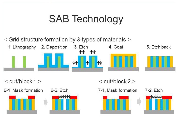
Fig. 5 SAB technology
