Research and Development
Research and Development for the Future
With the evolution of ICT, electronics are more and more indispensable to people’s lives. In addition, there is an increasing need to realize both the development of a data-driven society and preservation of the global environment, with the growing demand for semiconductors, which is the base of ICT and increasing global awareness of the environment. The performance required of semiconductors is also becoming more diversified.
In order to contribute to the development of a dream-inspiring society, Tokyo Electron is engaged in R&D with an eye on the future to capture changes in society, including innovations in manufacturing technology and the pursuit of ultra-efficient productivity.
Market Heading toward Diversification

CPU: Central Processing Unit. A semiconductor chip that serves as the brain of a computer.
Strengthening Research and Development Capabilities
To continuously create the high-value-added next-generation products needed for technological innovation in semiconductors and bring them to the market in a timely manner, we promote technological development and integration while domestic and overseas development sites, Business Divisions and the Corporate Innovation Division maintain their respective individuality and collaborate in necessary areas. We construct development systems ranging from fundamental technologies to mass-produced products and promote DX that uses AI technologies in our R&D.
Each development site and Business Division has an eye toward future generations and is engaged in the development of semiconductor production equipment with innovative technologies. They also promote R&D related to peripheral technologies for this production equipment.
The Corporate Innovation Division strives for the creation of further high-value addition by working closely with each development site to develop cross-function initiatives in each product area as well as promoting and optimizing R&D while maintaining a bird’s eye view on the entire development structure. In addition, the division is also engaged in a search for potential growth areas, as well as in R&D of fundamental technologies toward creating value in the future.

CSS: Composed of the Vice President and General Managers of Tokyo Electron, Presidents from overseas subsidiaries
Shift Left
We are focused on using the Shift Left approach, investing resources such as technology, personnel and expense into the early processes of product development. Through this approach, we are endeavoring to develop various technologies and conducting research for multiple future generations in order to realize the technology roadmaps we have created with customers.
With product development through the Shift Left approach, we understand customer needs at an earlier stage, reflect the information obtained from feedback into our R&D and propose superior products. This contributes to maximizing yield for customer devices and capacity utilization of their mass production line equipment. We are also promoting on-site collaboration for early delivery of evaluation equipment to customers’ fabs and development and research laboratories, and are working to accelerate the process in which R&D is reflected in mass production equipment as well as to optimize development efficiency.

Product Marketing
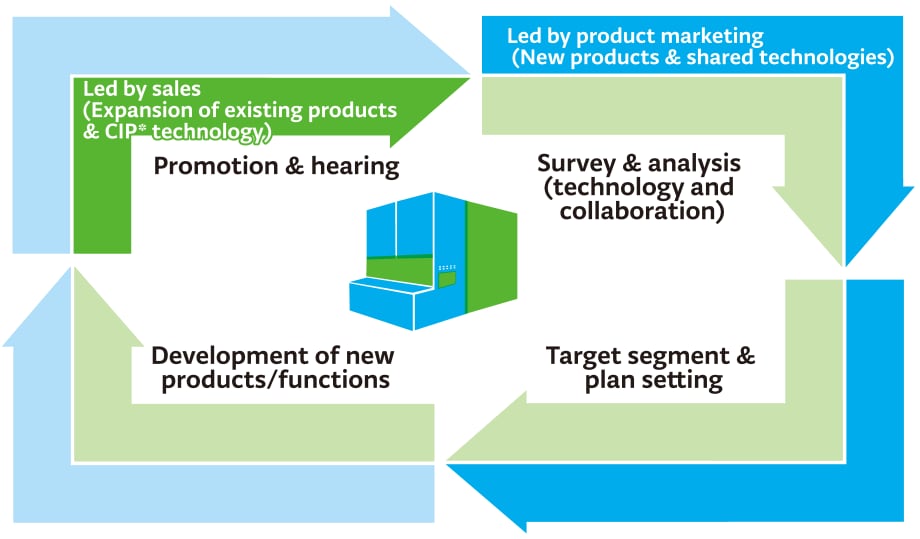
We are endeavoring to further enhance the productivity of product development by having our sales departments and product marketing departments appropriately fulfill their respective roles.
Our sales departments not only take responsibility for reliably delivering products and services to customers based on solid relationships of trust, but are also working to improve customer satisfaction levels still further by accurately gaging customers’ true needs and working in partnership with development departments on initiatives relating to the improvement and enhancement of products and services.
Meanwhile, our product marketing departments work to plan cutting-edge products that meet the future needs of customers in target markets, and roll out activities based on these plans. In addition to considering new products and functions based on the seeds created by our development divisions, our product marketing departments also formulate plans for optimal collaboration including tie-ups with partner companies and consortiums, to create products with still high-value-added.
In the semiconductor industry, where change happens at bewildering speed, companies need the flexibility to change policies in a timely manner as and when circumstances require. Our sales departments and product marketing departments work together in developing product marketing activities that anticipate market needs and contribute to customers’ products, and in doing so, help improve our product competitiveness and promote our Shift Left approach.
Roles of Sales Departments and Product Marketing Departments for Product Development

CIP: Continuous Improvement Program
Collaboration with Consortia and Academia
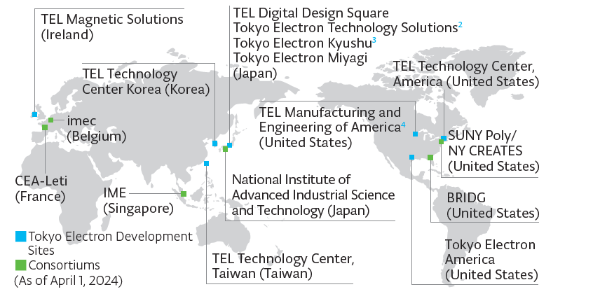
For many years, Tokyo Electron has been focusing on joint research and development efforts with domestic and international consortia and academia (universities). These initiatives include development under CHIPS Acts*1 that are currently being promoted in the USA and Europe to help develop infrastructure to maximize the benefits of open innovation-based development in each region. In recent years, we are also making efforts to boost human resource development in the semiconductor industry through collaboration with major universities in Japan and abroad.
We continue our engagement in a wide range of collaborations from applications to product development in various fields of semiconductor technology. R&D is of course underway in the front-end and back-end areas at TEL Technology Center, America, which marked its 20th anniversary in 2023. We also participate in a global research hub for hardware development of next-generation AI, leading-edge logic and quantum computing. Collaboration is also underway with imec in the field of EUV and high-NA EUV*2 patterning technologies and logic process development; and we have a partnership with BRIDG*3, a non-profit public-private partnership in Florida, USA.
With the diversification of semiconductor development, we collaborate with the National Institute of Advanced Industrial Science and Technology (AIST), one of Japan’s largest public research institutions, leveraging its world-class research environment and personnel to enhance our own development by conducting research in the MRAM*4 and 2D material-related research.
CHIPS Act: Creating Helpful Incentives to Produce Semiconductors and Science Act. An act to support investment in the USA into semiconductor development and mass production, AI, quantum computing and communications technology.
EUV and high NA EUV: Extreme Ultraviolet. A semiconductor industry term for an exposure technology that uses a specific wavelength of 13.5 nm. High-NA EUV refers to next-generation EUV, an exposure technology that shortens the resolvable line width by increasing the numerical aperture (NA)
BRIDG: A non-profit public-private partnership specializing in areas including deposition of III-V materials for advanced system integration, microelectronics manufacturing, sensors, optoelectronics and high-speed transistors
Magnetoresistive Random Access Memory. Magnetoresistive memory

Tohoku Office, Hosaka Office, Fujii Office
Koshi Office, Otsu Office
Chaska Office, Chelmsford Office
Intellectual property management
We are promoting intellectual property (IP) management under the fundamental tenet of contributing to an increase of corporate profits by supporting our business activities through IP protection and its utilization.
To achieve sustainable growth in the semiconductor industry where the growth is driven by technological innovation, we are globally expanding our R&D activity including industry-academia collaborations. IP professionals are assigned to headquarters, R&D, and production sites around the world to evaluate inventions created in R&D projects from various perspectives such as technology trends or marketing, and we have established IP portfolios aligned with our technology and product strategies.
In 2022, the number of inventions created in Japan was 1,226 and 317 in other countries. We have maintained the global patent application rate* approximately 70% for ten consecutive years, and the allowance rate of the filed patents has reached 74% in Japan and 81% in the United States. Furthermore, various inventions have been created through collaboration with domestic and overseas business partners, consortium, and academia, and we have jointly filed patent applications on 41 inventions in the past two years. Consequently, the number of active issued patents as of March 31, 2023 is 21,645, which is the largest number in the semiconductor production equipment industry, and we are building our competitive edge in the intellectual property field on a global level.
In recognition of these initiatives, we have been selected as one of the "Clarivate Top 100 Global Innovators 2023” for the second consecutive year. In this award, Clarivate, a global information service company, makes an original evaluation based on patent data, and once a year recognizes “companies or institutions protecting original invention ideas with intellectual property rights, and leading the world's business through successful commercialization”.
We strive to improve the competitiveness of our products through differentiating our own technologies with building a competitive IP portfolio in terms of both quantity and quality.

Global patent application rate: the percentage of inventions filed in multiple countries among the number of filed inventions as patent application.
