Yield Enhancement Technology: Efforts to Suppress Nanosized Particles in Semiconductor Production Equipment

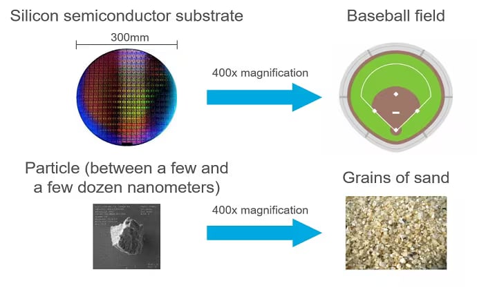
The currently dominant semiconductor process size is in the range between a few and a few dozen nanometers. That means if a nanosized particle smaller than a virus (hereinafter simply “particle”) is present on a silicon substrate, it could cause a defect in the semiconductor device, lowering the production yield (i.e., the percentage of good chips produced in a manufacturing process). Preventing the occurrence of defect-causing particles is not so easy, however, as it is comparable to cleaning up a baseball field until no grain of sand larger than a few dozen microns in diameter remains on the ground (Figure 1). Despite the difficulty, developers of semiconductor production equipment have continually struggled to suppress particles.

Figure 1. The proportion of a particle to a silicon semiconductor substrate is comparable to that of a grain of sand to a baseball field
One of the measures to suppress particles in semiconductor production processes is to use a clean room, which ensures that the concentration of airborne dust particles is reduced to a designated level under a temperature- and humidity-controlled environment. However, clean rooms alone cannot entirely prevent the occurrence of particles inside each unit of semiconductor production equipment. As Tokyo Electron (TEL) offers one of the largest portfolios of semiconductor production equipment in the world as their developer and manufacturer, the company has been studying measures to control the occurrence of particles in every one of its products, and has successfully developed a wide variety of innovative particle reduction technologies.

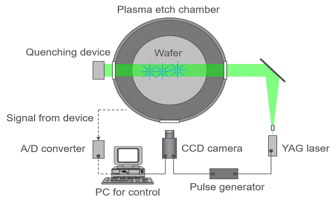
Figure 2. Experimental system for particle visualization integrated with a plasma etch system
For example, we conducted an experiment in which we irradiated particles generated in a plasma etch system with a high intensity laser beam, to observe the movement of particles within the system and determine the timing they were generated (Figure 2). The experiment led to the discovery of several previously unknown principles. We found, among other things, that particles are mainly generated under one of the following conditions: when gas enters the chamber; when pressure changes; when voltage is applied; when vibration occurs; and/or when temperature changes. Among these, changes in pressure were empirically known to generate particles, but the mechanism of this phenomenon had not been clearly understood before our experiment.
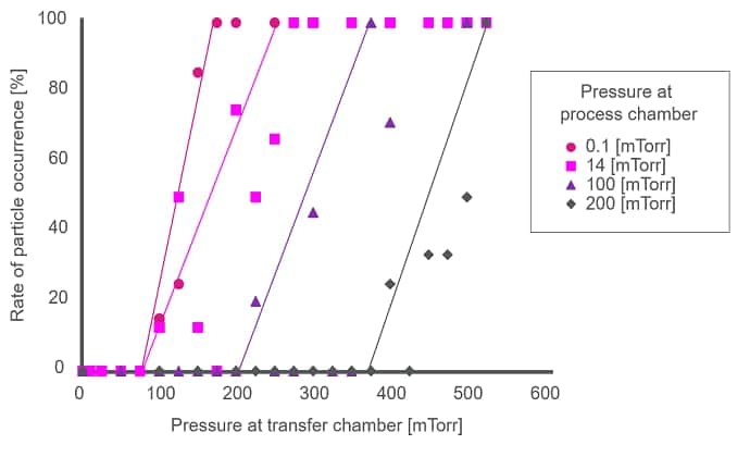
Our research into the relationship between particle generation and pressure changes also revealed something very interesting. Sudden pressure changes occur in a plasma etch system when the gate valve between the process and transfer chambers is opened. When the process chamber pressure is at or over 200 mTorr, particles are generated only if the transfer chamber pressure is twice that or more (Figure 3). We performed simulations based on this experiment and figured out that the occurrence of particles is triggered by shock waves. We also found that particle occurrences can be reduced by curbing the energy of shock waves[1].

Figure 3. Relationship between particle occurrence rate and chamber pressure when gate valve is opened
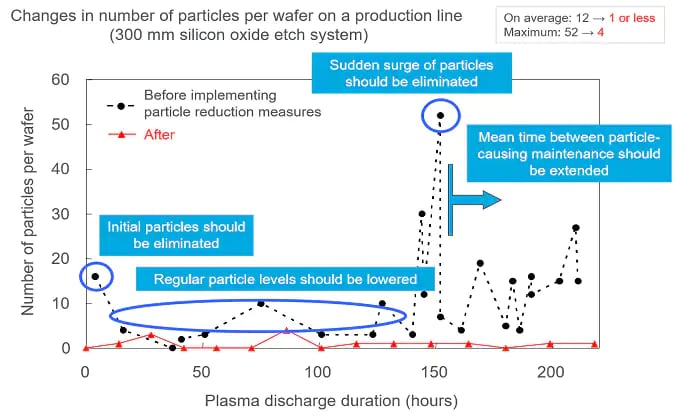
We also developed a technology for suppressing particles generated by turbomolecular pumps used in vacuum units for plasma etch and other systems[2], and a technology for reducing particles caused by faulty maintenance[3]. We then implemented a number of particle reduction measures in our plasma etch systems installed at semiconductor fabs, with the result that in one process, the average number of particles on a wafer was reduced from 12 (max. 52) to 1 or less (max. 4), which was a remarkable improvement (Figure 4). TEL has been sharing the information about these particle reduction technologies globally through academic presentations and papers, and has received three Best Paper Awards so far at the International Symposium on Semiconductor Manufacturing (ISSM).

Figure 4. An example of efforts to reduce particles in a plasma etch system
In a disaster such as an earthquake, semiconductor fabs could suffer severe damage. Once a cleanroom in a fab stops being operational, it is imperative not only to restore the building and facilities but also to bring particle concentration down to previous levels. TEL can help the recovery of disaster-stricken fabs back to production, repairing damaged semiconductor production equipment and quickly improving the yield by fully applying its proprietary particle reduction techniques[4].
TEL swiftly catches the most advanced technology trend at its principal development and manufacturing bases in Japan as well as its R&D facilities throughout the world, and works closely with world-leading semiconductor manufacturers to conduct joint R&D. Also, TEL is collaborating with global consortia and development partners and continues to explore breakthrough technologies to address various challenges in enhancing the productivity of semiconductor production equipment.
- References:
- [1] Particle reduction and control in plasma etching equipment, T. Moriya, H. Nakayama, H. Nagaike, Y. Kobayashi, M. Shimada and K. Okuyama, IEEE Trans. Semicond. Manufact., 18, 477 (2005)
[2] Observation and Elimination of Recoil Particles From Turbo Molecular Pumps, T. Moriya, E. Sugawara and H. Matsui, IEEE Trans. Semicond. Manufact., 28, 253 (2015)
[3] Using an Optical Motion Sensor for Visualization and Analysis of Maintenance Work on Semiconductor Manufacturing Equipment, M. Kagaya, S. Tanaka, H. Matsui, T. Moriya, IEEE Trans. Semicond. Manufact., 30, 333 (2017)
[4] Preventive Methods on Plasma Chamber Corrosions by Earthquake, T. Moriya (AVS, 2013)
